Atomic Manipulation
Manipulation of single adsorbed atoms and molecules, tip-induced molecular switching and conformational changes
The precise manipulation of individual atoms and molecules, made possible by the progress in scanning tunneling microscopy instrumentation and the development of various manipulation procedures, is a most fascinating and relevant task in nanoscale science. It allows not only to structure and modify matter on the atomic scale, but also grants access to basic physical properties of such artificial nanostructures. Typical examples from literature include the positioning of single atoms and molecules, induced chemical reactions, conformational changes in large organic molecules, atom-by-atom doping of fullerenes or the sequential uploading of metal atoms into a molecular “freighter”.

In order to assemble artificial CO structures we applied a lateral manipulation procedure, where the molecule is moved by interactions with the STM tip. A typical manipulation includes the following steps: i) the tip is positioned behind the target molecule and approached close to the surface by applying small bias voltages (50mV) and large tunnelling currents (80nA). ii) the tip is translated along a line towards the desired final position. Short range forces between the CO and the tip induce sudden hops of the molecule. These jumps from one lattice site to the next can be observed in the tip height. Figure c) shows the sawtooth trajectory of the vertical tip position while a CO molecule was moved over 12 lattice sites along a close-packed Cu row. iii) at the target position, the tip is again retracted by changing back to the imaging parameters. A subsequent image is taken to check if the manipulation was successful.
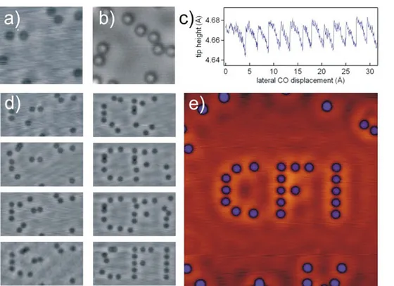
Panel a) shows the Cu(111) surface after a minute exposure to CO dosed in-situ at a sample temperature of 18 K. Each depression corresponds to a single CO molecule imaged with a bare metal tip. It is interesting to note that picking up a CO molecule by vertical manipulation changes the imaging mechanism completely (b). Additionally, the CO functionalized tips guarantee an increased resolution.
The image sequence displayed in panel (d) presents some snapshots during the writing procedure of the letters CFI. The high-resolution image (e) shows the final step of the manipulation process. Every blue spot is a single CO molecule adsorbed on an “on top” position of the underlying Cu substrate lattice. Thus, for example the separation of two CO molecules in the letter “I” is a mere 5Å. The successful assembly and imaging of this artificial nanostructure demonstrates the high stability and performance of our low-temperature STM setup.