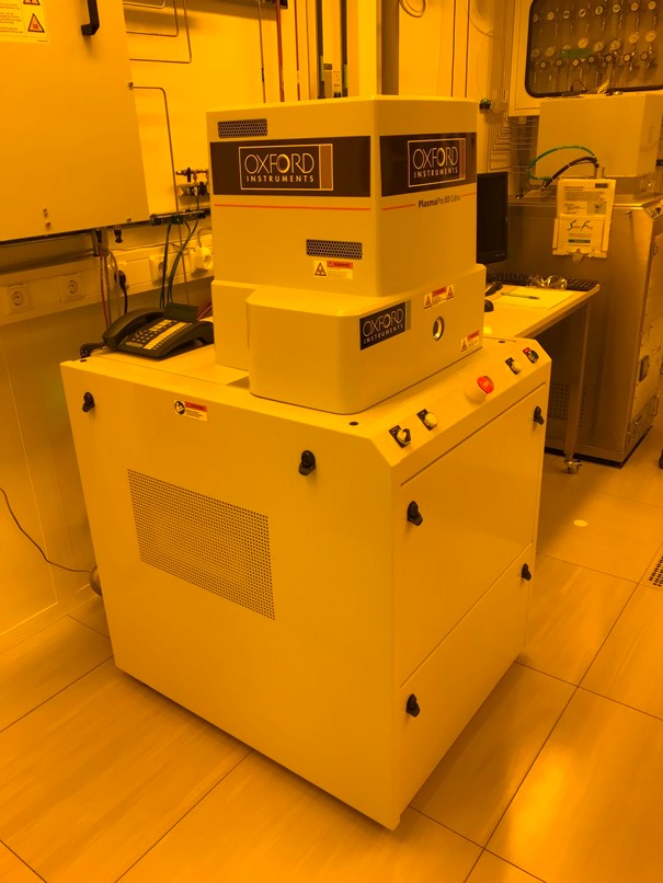
Oxford PlasmaPro 80 Cobra RIE
Configuration
The Oxford PlasmaPro 80 ICP can be operated in RIE (300 W, 13.57 MHz) and ICP (300 W, 13.57 MHz) mode with fluorine and chlorine chemistry. Installed gasses are: CF4 (50 sccm), CHF3 (100 sccm), SF6 (100 sccm), C4F8 (100 sccm), O2 (50 sccm), Ar (50 sccm), Cl2 (50 sccm) and BCl3 (50 sccm). Pressures are measured using a Penning gauge and a 100 mTorr CM gauge. The system can in principle etch wafers up to 100 mm, but is designed to work with small samples as the ICP has a 65 mm diameter. The temperature of the sample platen can be set in the range of 0 - 80 oC, and thermal contact can be improved using helium backing.
How to get access?
The machine in part of the ZNN cleanroom and in principle all users can get access to the machine. This list will guide you through the different steps to take if you want to use the etcher.
- Fist ask yourself: What processes do you want to do? Is this possible with the machine? Are all materials allowed? Did you work with a plasma etcher before? Once you have a clear idea about these points, discuss them with us.
- Get access to the ZNN cleanroom. This requires introductions and safety trainings. However, without access to the cleanroom, you cannot proceed to the next step.
- Fill out and sign the form for requesting access. Let your supervisor sign it.
- Make an appointment and follow the general introduction to the machine with one of the supervisors.
- Practise a number of times with the machine.
- Demonstrate your ability to independently operate the machine to a supervisor
Only after successfully passing step 6, you will get a login and will be allowed to use the machine by yourself. Note that for e.g. operation with chlorine gasses, additional training is required.
Allowed materials
To prevent cross-contamination and to keep the system in a usable state for all users, not all materials can be allowed in the etcher. In general, no magnetic materials are allowed, and metals are handed on a case-by-case basis and if allowed, then typically only in small quantities. CMOS compatible materials (Si, SiN) are usually OK. Once you have access to the ZNN and its Wiki, check the table if the material that you want to etch is allowed and read the explanation below it. Note that "Etching allowed" does not mean that you can do anything you want. Certain processes, such as the Bosch process, or etching more than 1 um are in general not allowed to safeguard the well being of the etcher. Also, keep in mind that there may be additional rules (e.g. materials not allowed, MSDS requirement) imposed by the ZNN cleanroom.
When a material is not listed, contact a supervisor to discuss the possibilities. This list will be updated regularly so remember to check it regularly. We reserve the right to remove materials from this list if these turn out to interfere with other user's processes, or are bad for the equipment.
Acknowledgement
This system has been acquired with support from the Nanosystems Initiative Munich (NIM) and TUM-IAS. We thank everybody for their relentless efforts to keep the system running. Make sure to thank the superusers for their time, everytime you see them. Happy etching!