Equipment
Measurement equipment


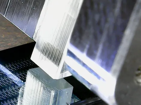
Our group works has extensive experience with measurements on integrated optics devices. The lasers that we use are typically tunable semiconductor lasers that operate at telecom wavelengths (around 1550 nm), but other wavelengths are also used. The laser light is sent onto the chips using a fiber array that is positioned above the grating couplers of the device under test. Locating the device and optimizing the position can be done fully automated, enabling rapid, reproducible characterization of the devices. This is aided with sweep lasers, low-noise detectors and fast data acquisition systems. Besides such optical measurements, also electrical signals can be applied to the devices via DC and microwave probes, for example to excite mechanical resonators, or to program an integrated quantum circuit.
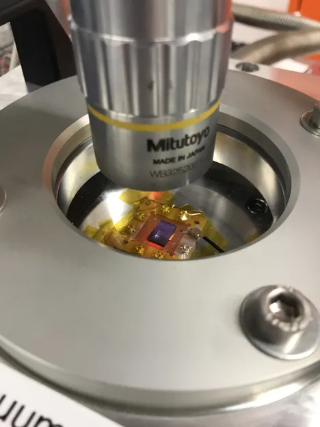
The measurements on mechanical systems are typically done in vacuum, to minimize the damping due to the surrounding air. For these, dedicated vacuum chambers with in-situ sample positioning are available, both for on-chip and for 2d optomechanics. Both types of mechanical devices operate at high frequencies (100 kHz - 10 GHz) which requires spectrum and network analyzers that can reach these frequencies. For feedback experiments, a fast lockin amplifier with multi-frequency and real-time options is available.
Our integrated quantum optics chips contain superconducting single-photon detectors which have to be cooled to temperatures close to the absolute zero. This is done in dedicated cryostats with electrical and fiber access. To measure such detectors, fast oscilloscopes and low noise sources are available.


Nanofabrication
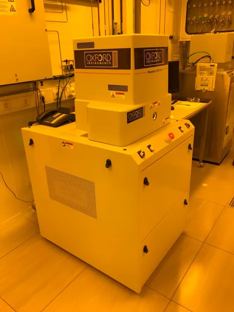
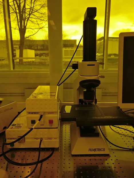
Making state-of-the art chips using advanced nanofabrication techniques is a major part of our research. This is carried out in close collaboration with the Walther Meißner Institute for Low Temperature Research (WMI), the Walter Schottky Institute (WSI), and its Center for Nanotechnology and Nanomaterials (ZNN). The reactive-ion etcher and microscopic reflectometer that we operated will continue to be accessible to users of the ZNN cleanroom.