Tunneling Spectroscopy

Besides imaging the surface topography, an STM system is also capable of extracting valuable information on the local electronic structure of clean and adsorbate covered surfaces by means of Scanning Tunneling Spectroscopy (STS) measurements typically at low temperature.
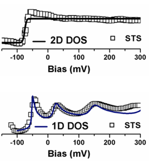
Local tunneling spectra are taken with the feedback loop open after stabilizing the STM tip at a given constant height above the surface. The bias voltage V is modulated (typical amplitude 3-20mV) at frequencies of a few hundred Hz while the differential conductivity dI/dV signal is recorded via lock-in detection. The figure below shows two spectra representing the steplike onset of the surface state band on a bare Ag(111) surface (top) and the modified electronic structure upon one dimensional confinement (bottom) respectively.

Two-dimensional maps of the conductivity (dI/dV maps) are often recorded simultaneously with constant current topographic images, where the value of the tunneling bias V is chosen in a way to highlight a specific electronic state.
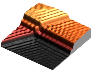
The image below represents a dI/dV map overlaid with a topographic image: As a result one can clearly recognize the standing wave pattern of surface state electrons scattered at the step edges.