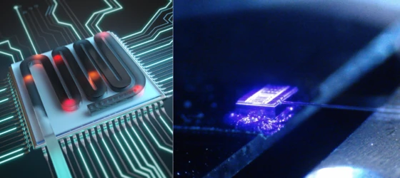
One major research focus of our group is the integration of erbium dopants into silicon host crystals to develop scalable quantum network nodes that leverage the technological maturity of silicon nanophotonics. This approach enables the fabrication of compact, robust quantum devices using wafer-scale nanofabrication techniques.
In a pioneering study, we demonstrated that erbium atoms can be reproducibly implanted into silicon at well-defined lattice sites, exhibiting properties highly favorable for quantum networking. These include strong optical transitions, inhomogeneous broadening below 1GHz, and remarkably narrow homogeneous linewidths-indicative of exceptional optical coherence-that persist up to 8 K [1].
Building on this breakthrough, we showed that erbium emitters can be reliably integrated into low-loss silicon waveguides produced by a commercial photonic foundry. This confirms the compatibility of these novel erbium sites with standard wafer-scale fabrication processes [2].
In addition to integrating erbium into silicon, a key part of our research is understanding the nature of the erbium integration sites themselves. Recently, we managed to identify the site symmetry and reconstruct the spin Hamiltonian for one of these newly discovered sites. These results help pinpoint the precise location of the erbium atoms within the silicon unit cell - an important step toward a microscopic understanding of erbium in silicon [3].
Our current research builds on these foundations, using ensembles of erbium dopants in silicon to explore chip-based quantum memories, thermometry, microwave-to-optical transduction, and further unravel the nature of erbium integration sites.
In addition, our group investigates single erbium dopants in silicon to build scalable quantum information processors. Such processors rely on highly efficient spin-photon interfaces, typically implemented using optical cavities. This represents one of two efforts to build quantum networks using individual erbium dopants. In contrast to the second approach which is based on open-microcavities and macroscopic membranes of some host crystals, we again aim to leverage the unmet nanofabrication and integration capabilities of the silicon nanophotonics platform.
We design and fabricate nanophotonic resonators with quality factors exceeding 105 and mode volumes smaller than a cubic wavelength resulting in very large Purcell factors. Such strong light-matter coupling opens the door to fast and coherent spin-photon quantum gates, which are key building blocks for distributed quantum computing and quantum networks [4].
Our first experimental results show that in a single spin-photon interface several spins can be individually addressed by spectral multiplexing. These emitters exhibit Purcell enhancements of up to 180, resulting in the shortest optical lifetime observed to date for a single erbium dopant (~800 ns). Furthermore, we demonstrated spin-resolved excitation of individual emitters and single-photon emission, optical Rabi oscillations, spin initialization, coherent spin rotations and optical single-shot spin readout [5].

Building on these results, the group continues to work on efficient spin-photon interfaces based on single erbium in nanophotonic cavities to facilitate entanglement generation between erbium spins and telecom photons and between remote erbium spins.
[1] A. Gritsch et al., Narrow Optical Transitions in Erbium-Implanted Silicon Waveguides, Phys. Rev. X 12, 041009
[2] S. Rinner et al., Erbium emitters in commercially fabricated nanophotonic silicon waveguides, Nanophotonics, vol. 12, no. 17
[3] A. Holzapfel et al., Characterization of the Spin and Crystal Field Hamiltonian of Erbium Dopants in Silicon, Adv. Quantum Technol. 2024, 2400342
[4] A. Gritsch et al., Purcell enhancement of single-photon emitters in silicon, Optica 10, 783-789
[5] A. Gritsch et al., Optical single-shot readout of spin qubits in silicon, Nature Communications 16, 64
