Research
Photoelectrochemical energy conversion is a promising approach to convert solar energy directly into storable, energy-dense fuels. Our research focuses on revealing reaction mechanisms and interfacial processes on semiconductor-based multilayer photoelectrodes for solar energy conversion. In particular, we aim to understand fundamental reaction processes at their relevant length scales. To this end, we employ advanced scanning microscopy techniques to locally probe the material properties and stability under realistic operation conditions and at the nanoscale. The gained knowledge will be applied to engineer photosystems with improved efficiency and stability.
Understanding dynamic processes at nanoscale working interfaces
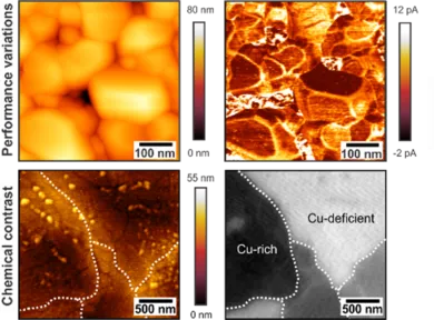
Photosystems are often composed of polycrystalline or nanostructured materials with highly complex architectures, which can lead to local variations in the material properties and impact the performance of the macroscale device. In our group, we aim at resolving local heterogeneities within semiconductor thin films to understand their fundamental material properties at the nanoscale.
In a recent study on bismuth vanadate thin films, we demonstrated the tolerance of charge transport to grain boundaries by correlating morphology and local optoelectronic properties under ambient conditions and illumination. The transport across single grains is space charge-limited and impacted by surface adsorption of gaseous products.
In copper vanadate thin films, we resolved variations in the local chemical composition and their correlation to macroscopic photoelectrochemical properties. The gained insights revealed deleterious effects on the photocatalytic activity and stability that are otherwise not apparent from pure macroscopic characterization.
Related publications
J. Eichhorn et al., ACS Appl. Mater. Interfaces, 13, 23575 (2021)
J. Eichhorn et al., Small 16, 2001600 (2020)
J. Eichhorn et al., ACS Appl. Mater. Interfaces, 10, 35129 (2018)
J. Eichhorn et al., Nature Commun., 9, 2597 (2018)
Efficient and stable interfaces for solar energy conversion
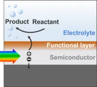
For solar energy conversion, we explore transition metal nitride semiconductor thin films as photoelectrodes using a well-controlled synthesis approach. The small bandgaps, good charge transport properties, and high tolerance to structural defects renders nitride material as highly interesting for solar water splitting. Specifically, we elucidate the fundamental semiconductor properties as well as the impact of defects on its optoelectronic characteristics, photoelectrochemical properties, and photocarrier transport. Particular challenges of water splitting devices are the poor efficiency and instability of the semiconductor photoelectrodes under the harsh photoelectrochemical operation conditions. A promising strategy to overcome these limitations is by protection/passivation of the semiconductor surface with conformal functional layers.
Recently, we designed ultra-thin catalyst layers with tailored structural, mechanical, optical, and electrochemical properties by leveraging non-saturated oxidation conditions in plasma enhanced atomic layer deposition. Since no protection layer or engineered interface is perfect and local imperfections can lead to complete device failure, we also investigate new design strategies of multilayer devices. To this end, we aim to combine conformal, ultra-thin protection layers with local self-passivation of the photoelectrodes as an integrated self-protection mechanism to engineer truly stable photosystems.
Related publications
M. Kuhl et al., Adv. Mater. Interfaces 2022, 9, 2200582